
FEMTOSECOND LASER DIRECT WRITING
Solution for ultrafast manufacturing workstation
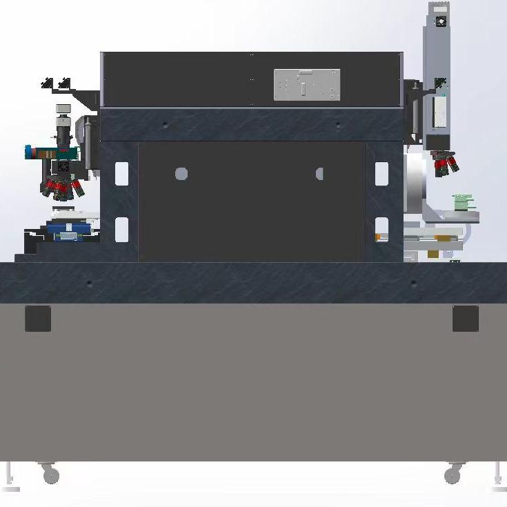
Industrial
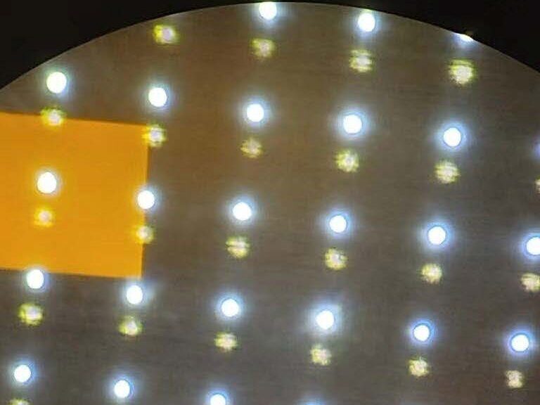
Parallel multi-beam projection processing system,High precision and high throughput,Arbitrarily complex 3D patterns,TGV processing
Scientific
Customize the system according to the application, which has high repeatability. The CPA technology femtosecond light source is suitable for a wide range of material processing.
Professional
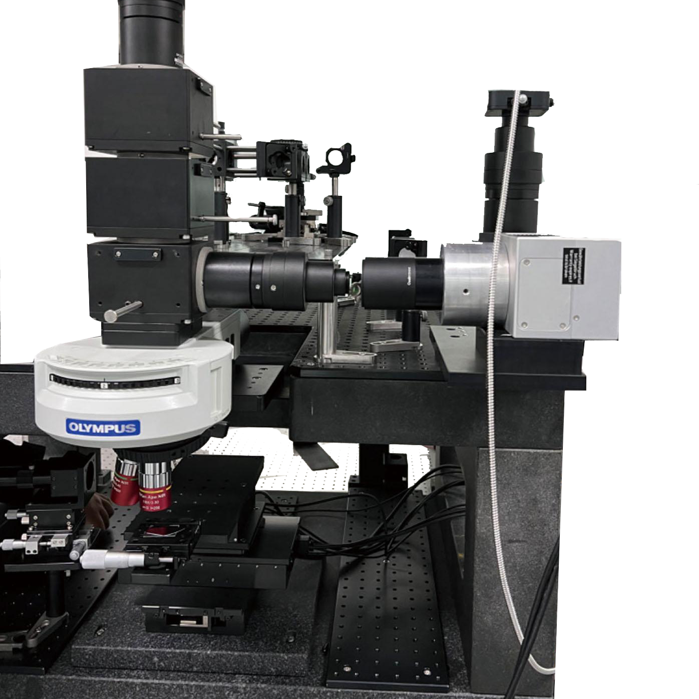
We optimize the system in TGV manufacturing, optical waveguide direct writing, FBGs. Assemble suitable sample fixtures and cups, focus feedback control, fiber core scanning, autofocus and other functions
Commercial System!
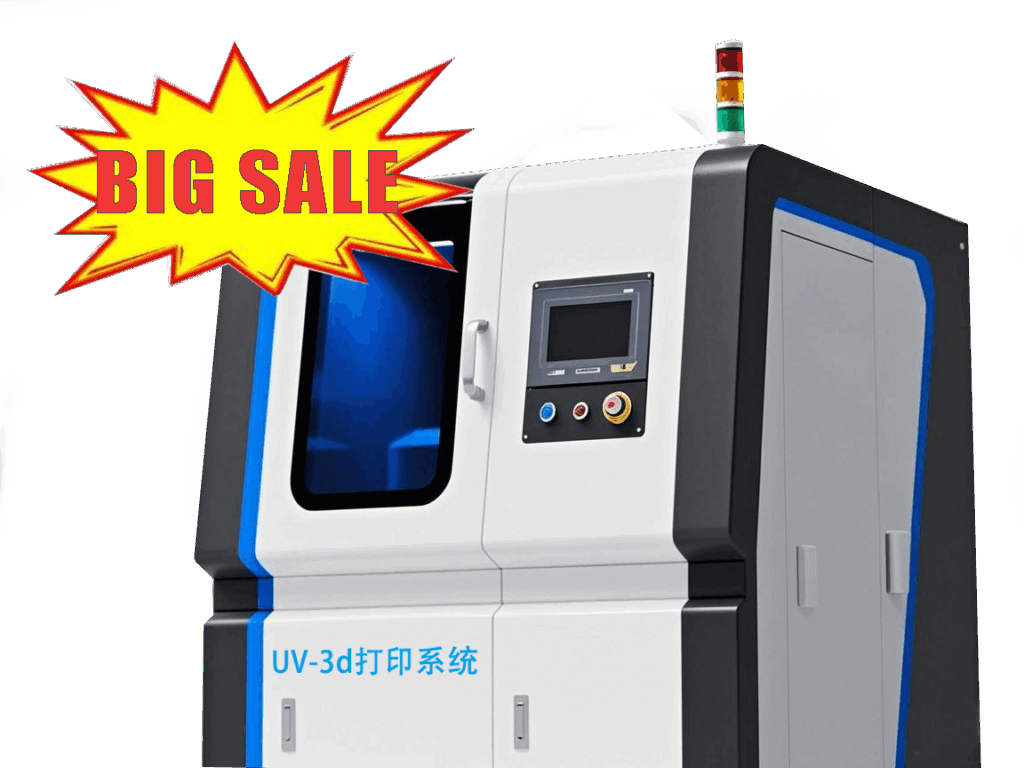
UV-3D Printing System
System features 0.5µm resolution, 405 nm LD laser. It handles 150×150 mm structure,Rapid manufacturing of large-sized buildings,Stage (X/Y/Z/θ motion)…….
Only $100,000!
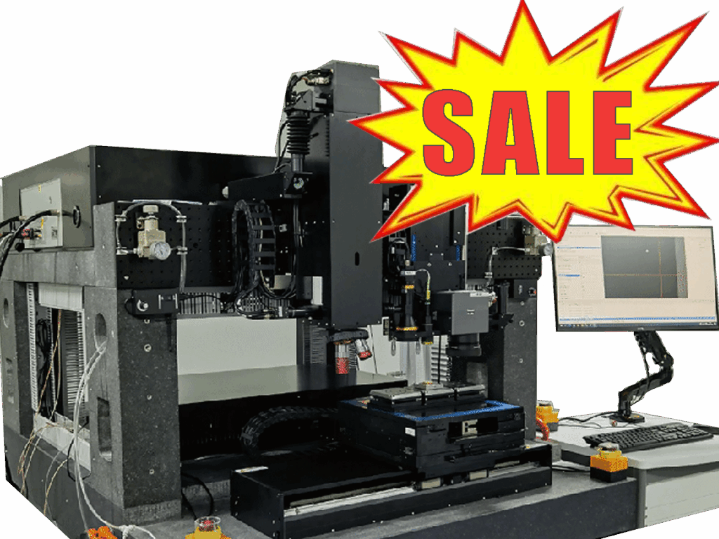
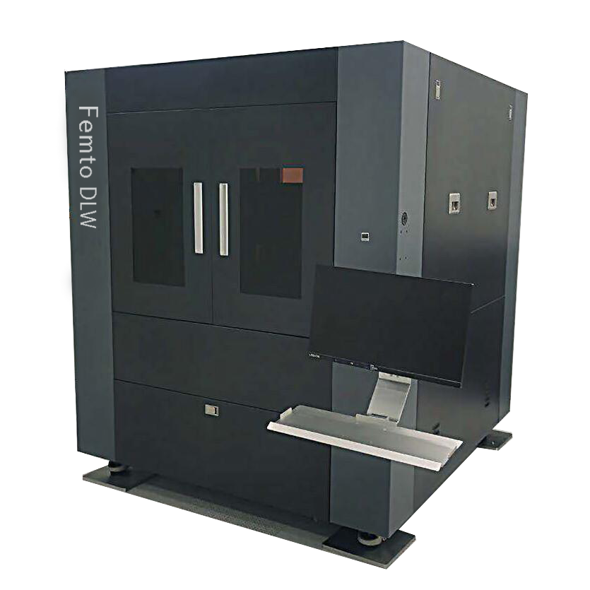
Femto DLW Gen 3
Assembling a solid-state Femtosecond laser, 100uj@100KHz ,XYZ repeated positioning accuracy can reach 100nm, with automatic focusing……
Only $200,000!
Product
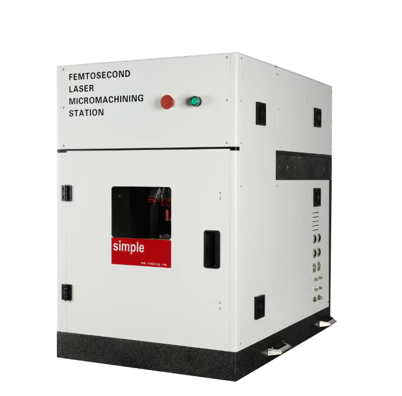
The Kit system for femtosecond laser processing, start your experiment…….

Customized system for scientific research, providing process parameter assistance ……
Flexibly build aligned customer laboratories, if you have femtosecond laser light sources……
Professional TGV and Microfluidic Chips manufacturing system……
Industrial series large stroke processing system, capable of completing large……
High throughput Femtosecond laser holographic parallel multi-beam ……

Focused on femtosecond laser processing induction and observation……
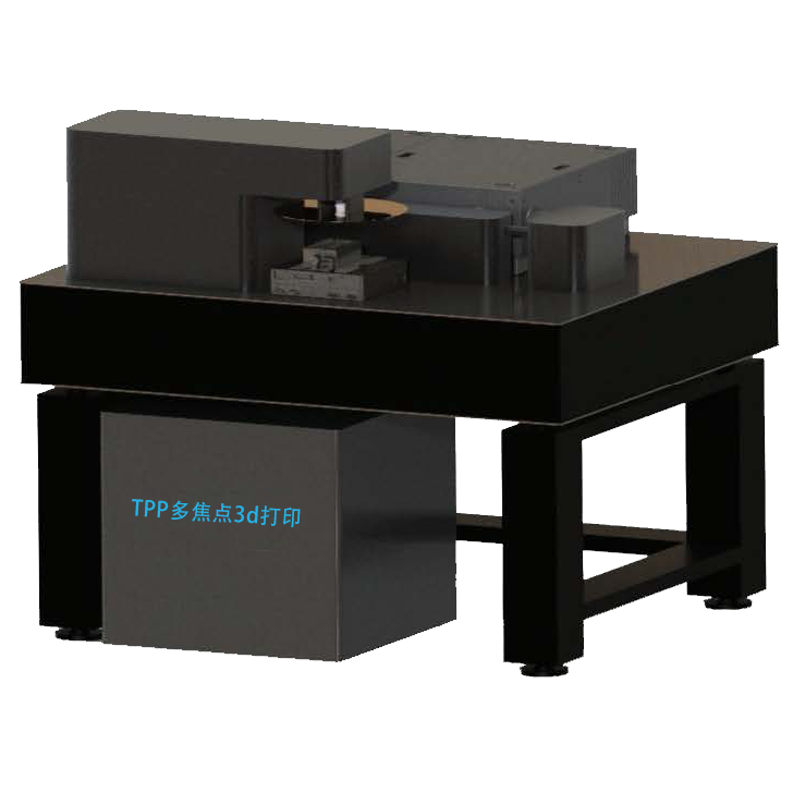
True 3D holographic manufacturing system, individual control of any focal point ……

Large volume buildings and fast UV direct writing applications……
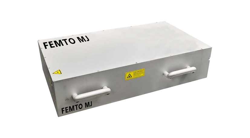
Featuring optimized gain media and cavity design, it delivers millijoule-level pulses ideal for laser processing, precision cutting ……..
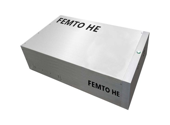
It delivers stable, high-frequency output ideal for ultrafast spectroscopy, imaging, and microstructure fabrication—supporting …….
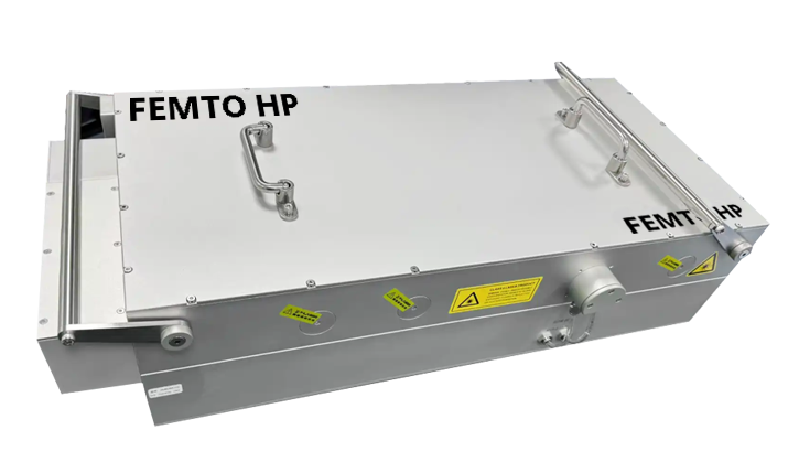
Specifically designed for high-power three-photon microscopy, this laser delivers up to 40 W output with low noise and high …….
ABOUT US
We focus on micro nano manufacturing systems, with building sizes ranging from hundreds of nanometers to hundreds of centimeters. We are committed to becoming experts in micro nano manufacturing, optimizing our systems to make them easier to use and industrialize, providing high-precision micro/nano fabrication solutions for optics, electronics, and biomedical fields.
Our company is incubated in a research institute, and our technical team has patented femtosecond laser technology and high-precision TPP projection printing technology. We are committed to recommending micro and nano manufacturing solutions from China to the world.
Contact us, get a quotation!
Scientific research and industrial
1)TGV
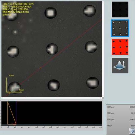
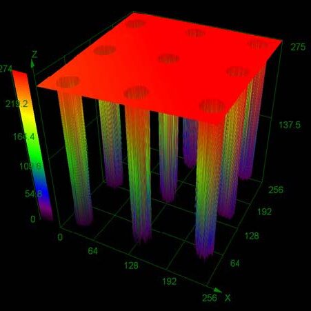
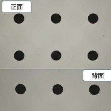
- Silicate Glass TGV Through-Hole, 30μm Hole Diameter, 300μm Depth, 100μm Pitch
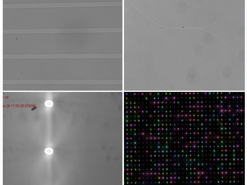
2) Fiber Bragg Grating (FBG)
3)Surface Removal
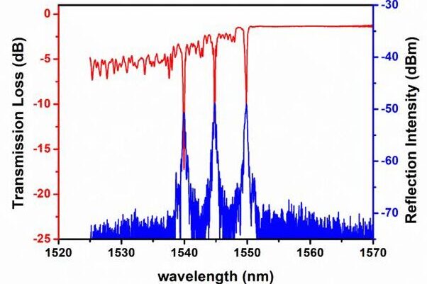
- Wavelength Range: 1540-1545-1559nm (Pi fiber)
- Side Mode Suppression Ratio (SMSR): > 10 dB
- 3dB Bandwidth: < 0.6 nm
- Reflection Rate: > 90%
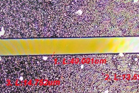
- Removal of Chromium Coating on Photomask Surface with 5 μm Linewidth5μm
- Chromium Layer Thickness: 300 nm; No Damage to Glass Substrate
4)Waveguide Chips
5)Medical devices
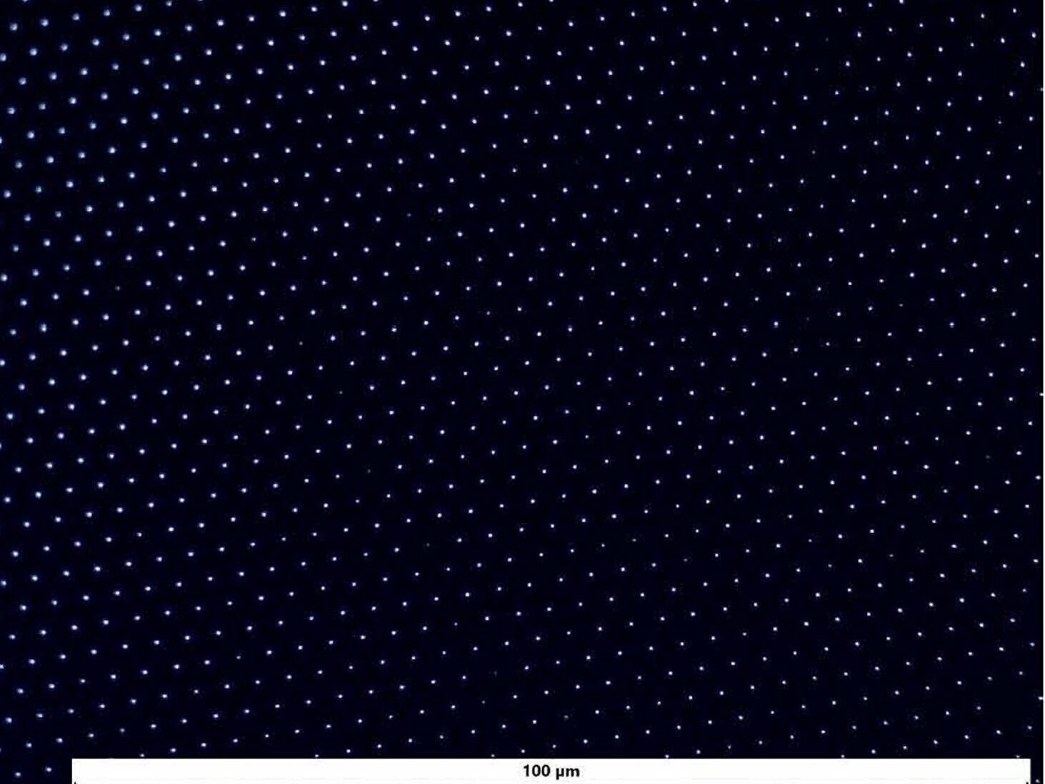
- High-Density, High-Precision Metal Micropore Array Filters
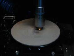
6)TPP Printing
7)Metasurface Etching

- 3D-Printed Microrobotic Components3D
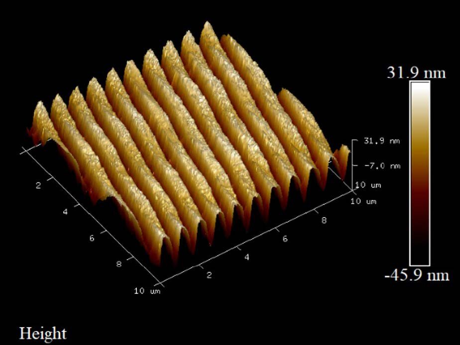

- Uniform Fine Etching of Silicon Wafers: Nanograting Grooves with a Linewidth of 365 nm and a Depth of ~30–40 nm
- Nanograting Etching on JGS1 Fused Silica Glass